Instruction Parameters
Supported PLC Series
| PLC-AES | PLC-FB | PLC-ES |
|---|---|---|
| ✓ | ✓ | ✓ |
Supported Data Registers
| M | X | Y | K | L | F | T | C | S | Z | R | Q | D | @D | Constant | |
|---|---|---|---|---|---|---|---|---|---|---|---|---|---|---|---|
| S1 | ✓ | ✓ | ✓ | ✓ | ✓ | ✓ | ✓ | ✓ | – | ✓ | ✓ | ✓ | ✓ | ✓ | – |
| S2 | ✓ | ✓ | ✓ | ✓ | ✓ | ✓ | ✓ | ✓ | – | ✓ | ✓ | ✓ | ✓ | ✓ | ✓ |
| D | ✓ | – | ✓ | ✓ | ✓ | – | ✓ | ✓ | – | – | – | ✓ | ✓ | – | – |
Supported Flags
| Flag | Bit | Support |
|---|---|---|
| Error | F11.0 | ✓ |
| Zero | F11.1 | – |
| Carry | F11.2 | – |
Number of Steps
| Steps |
|---|
| 4 |
Operands
| Operand | Description |
|---|---|
| S1 | The first operand. Entries are only WORD data registers. This is the location of the data register to read a BOOL value from. |
| S2 | The second operand. Entries are only WORD data registers. This is the bit number to read of the data register, S1. The value range is 0 ~ 15. |
| D | The third operand. Entries are only BOOL data registers. This is the bit address of the data register to write the value read from the data register, S1. |
Notice
Error Flag (F11.0) Notice
The error flag, F11.0, will be ON for one scan when the address of the data register assigned by @D exceeds the range of the data register, D. The range of the data register, D, is dependent on the CPU type.
Instruction Behavior
The TEST and TESTP instructions behave as follows:
- The value, S2, is value from 0 ~ 15.
- If the value, S2, is greater than 15, the remainder of S2 ÷ 16 is the equivalent.
- Example: if S2 = 17, the remainder is 1. This is the same as S2 = 1.
- If the value, S2, is greater than 15, the remainder of S2 ÷ 16 is the equivalent.
- If the BOOL data register, D, is 0, the status of the BOOL data register, D, is OFF.
- If the BOOL data register, D, is 1, the status of the BOOL data register, D, is ON.
Ladder Diagram Examples
TEST

The TEST instruction reads a BOOL value from the WORD data register, S1, at the bit number, S2, and saves the result in an assigned BOOL data register, D.

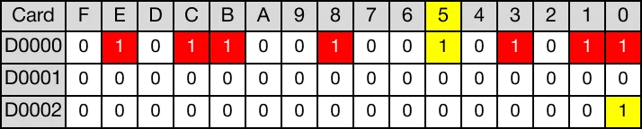
When the contact, M0.0, is powered ON (1), the TEST instruction examines the 5th bit of the data register, D0.

Since bit 5 is 1, the result BOOL data register, D2.0, is set to 1.
Memory Monitor
TESTP

The TESTP one-shot instruction reads a BOOL value from the WORD data register, S1, at the bit number, S2, and saves the result in an assigned BOOL data register, D. Every time this instruction executes, it energizes the output only once.

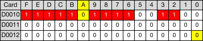
When the contact, M0.5, is powered ON (1), the TESTP instruction examines the 10th bit of the data register, D10.

Since bit 10 is 0, the result BOOL data register, D12.0, is set to 0.
Memory Monitor